Samsung J7 Max Circuit Diagram
3d samsung galaxy j7 model Samsung galaxy j7 (2018) (j737a) diagram [download 25+] samsung j7 schematic diagram free download – telegraph
Samsung Galaxy J7 Prime 2 SM-G611F schematics
Download samsung galaxy j7 j700f schematic diagram and service manual User manual samsung galaxy j7 (english Samsung galaxy j7 prime cell phone screen repair light problem solution
J7 schematic diagrama gsm
Smartphone repair, cell phone repair, mobile phone repair, sony mobileSamsung j7 prime 2 schematic diagram Schematic diagram samsung j7 primeJ7 schematics galaxy.
Samsung s7 circuit diagramSamsung j7 diagram schematic galaxy j700f manual service Samsung sm j700f schematic diagramSamsung galaxy j7 max motherboard pcb module.

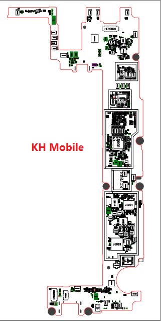
Laptop diagram: samsung j7 nxt schematic diagram pdf
Samsung j7 prime 2 g611f disassembly motherboard schematic diagramOriginal samsung j7 max charging logic price in bangladesh -etel Samsung j7 manual prime g610f sm service jmhSamsung j7 prime 2 schematic diagram.
J701f samsung j7 galaxy sm schematics coreSamsung j7 max, j7 pro, j7 prime, on nxt all similar disassembly [39+] samsung j7 max schematic diagram gsm forumSamsung galaxy j7 2016 j710f schematics.
[download 25+] samsung j7 schematic diagram free download – telegraph
Samsung j700f circuit diagram3d realistic samsung galaxy j7 model Samsung galaxy j7 prime 2 sm-g611f schematicsSamsung j7 max schematic diagram pdf.
Ways j7 g610f backlight jalur j2 jumper antena u2ugsm diagrama kunjungiSamsung j5 circuit diagram Samsung j7 prime pinoutDuo j7 schematics.

Samsung diagram device j7 galaxy att
In this article, “samsung galaxy j7 prime g610m display light ways lcdSamsung j7 max charging problem 💯 solution !! samsung j7 max charging Samsung galaxy j7 core sm-j701f schematicsSamsung galaxy j7 duo sm-j720f schematics.
Samsung j7 prime (sm-g610f) service manualSamsung galaxy j7 v user manual pdf download J7 max charging problemSamsung j7 schematic diagram pdf.

Schematics j7 j710f j710 motherboard j2 j5 sơ đồ phonelumi
Samsung j701f schematic diagramJ7 samsung max teardown prime .
.


